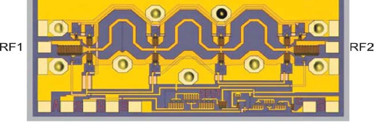
High-isolation, broadband, nonreflective SPST switch
The switch is based on a 0.18-lm GaAs pHEMT process.
Design
A parasitic drain-to-source capacitance limits the high frequency
isolation of the off-state transistor. A distributed topology
is adopted to extend the operating frequency band. The
shunt mounted transistors are connected through the series
high-impedance lines, such that the combination of the series
high-impedance lines and the shunt transistor off-state
drain-to-source capacitance form a 50 ohms artificial transmission
line. Thus, this structure has a low insertion loss in the frequency
range of operation.
The switch isolation is provided by the on-state shunt transistors
at high frequencies. At the same time, the off-state series
transistors provide low-frequency isolation.
Performance
The chip size is 2x1 mm2.
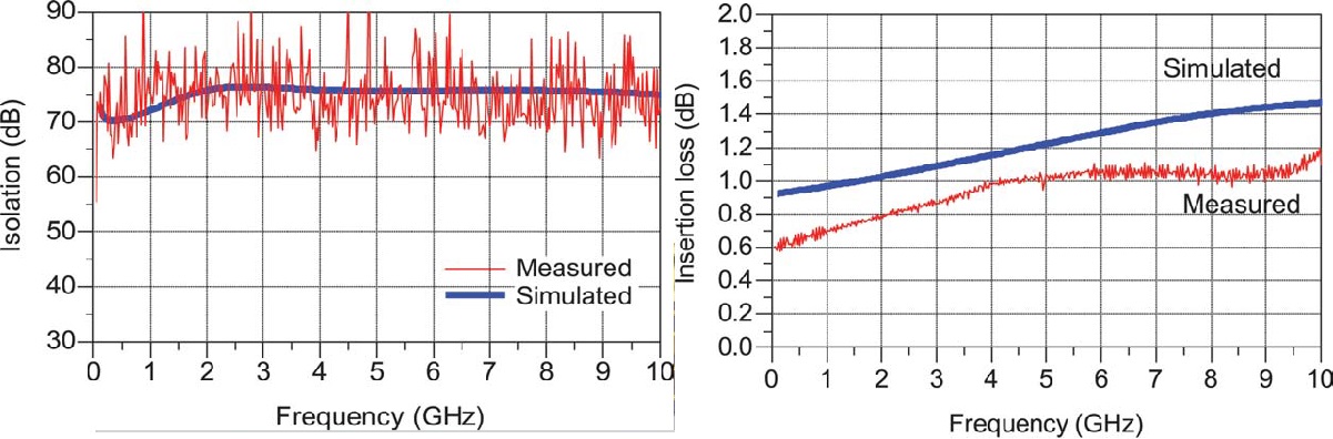
The measured on-wafer insertion loss is below 1.2 dB to 10 GHz. The isolation is typically better than 70 dB to 10 GHz. Unfortunately, the measured isolation is affected by the dynamic range of the measurement setup.
The 1 dB compression
point of the insertion loss is at 12 dBm input power, whereas
the isolation degrades by 5 dB. The input-referred third-order
intercept point is estimated to be 31 dBm.
The magnitude of S11 is below -16 dB in
on-state and -9 dB in off-state to 8 GHz.
Further details
can be found in this .pdf: DOI: 10.1002/mop.25906